Energy-Efficient HYbrid MEmory based Architecture for NeXt-Generation AI Systems
Links: [JSPS KAKENHI]│[PI’s Researchmap]│[Project Database]│[Project Page (under construction)]
Information
- Funder: KAKENHI (Grant-in-Aid for Scientific Research B)
- Project No: 26K02883
- Duration: 2026/04-2029/03
- Budget: 18,330,000 JPY
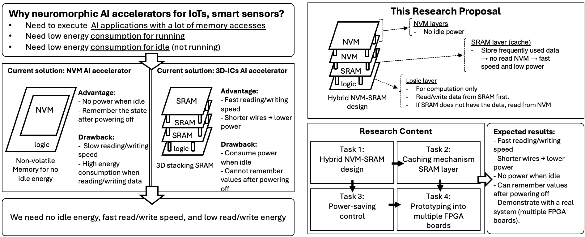
- Summary: Artificial Intelligence (AI) has made great progress, but its high energy consumption remains a serious challenge, especially for small devices such as smartphones, IoT sensors, and battery- or solar-powered systems. This project proposes a new energy-efficient neuromorphic AI accelerator using 3D integrated circuits (3D-ICs) that combine Non-Volatile Memory (NVM) and SRAM to reduce power usage both during operation and idle periods. NVM can retain data without power, significantly lowering idle energy consumption, but it is typically slower and more energy-intensive during read/write operations than SRAM. To address this, we introduce a hybrid memory architecture in which stacked NVM layers are placed above the logic layer to shorten data transfer distance, while a small, fast SRAM layer acts as a cache between logic and NVM to improve speed and reduce read/write energy. In addition, adaptive power management techniques dynamically adjust energy usage based on available power with minimal impact on accuracy and performance. With these technologies, the proposed design aims to reduce energy consumption during operation and during idle time, enabling practical low-power AI chips for real-world applications such as smartphones, IoT devices, and smart sensors.
Research Technology & Prototyping
Our research group specializes in the design and validation of high-efficiency AI hardware and next-generation memory-compute systems. We leverage industry-leading AMD (formerly Xilinx) FPGA platforms to bridge the gap between architectural theory and physical silicon realization.

Core Methodologies
Full-System Prototyping: We utilize a rigorous RTL-based design flow (Verilog/VHDL) within the AMD Xilinx environments. This ensures cycle-accurate hardware validation and reliable performance benchmarking for complex neural accelerators.
3D-IC & Interconnect Emulation: Recognizing the challenges of iterative 3D-IC fabrication, we use Network-on-Chip (NoC) features to simulate high-bandwidth vertical interconnects and through-silicon via (TSV) latency characteristics.
Advanced Memory Modeling: Our group develops custom behavioral wrappers to model the timing, energy signatures, and data-retention properties of emerging technologies, such as Non-Volatile Memory (NVM) and hybrid 3D-stacked SRAM-NVM.
NOTE: The final program will be released in Github under MIT license in the future.
Team Members
Students
AY2026
- HANYU Yuga
- SHARMA Atharv
- LUYEN Van-Vu
- KOMATSUZAKI Aruki
Schedule
Early Prototyping (Prior AY2026)
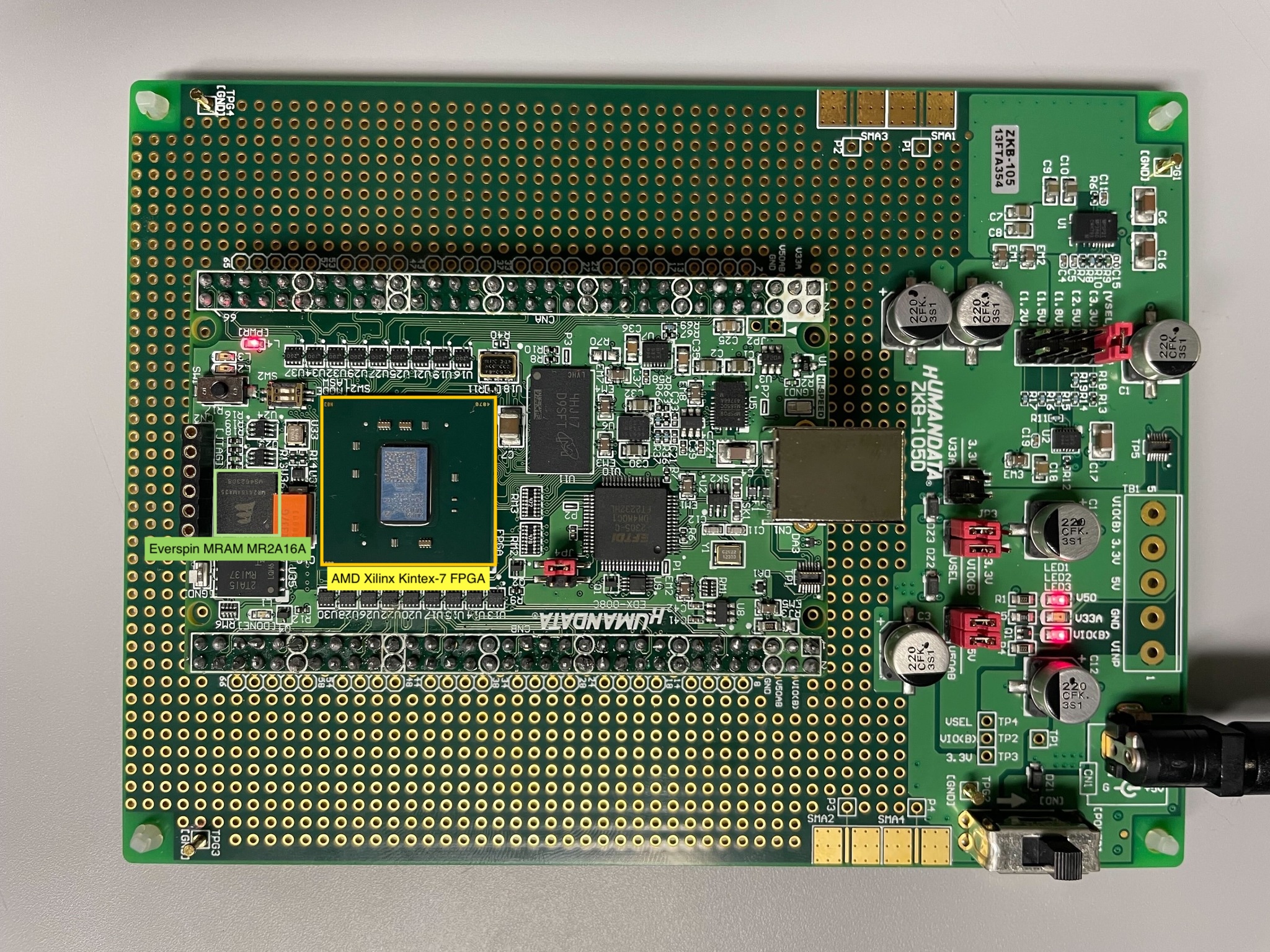
As a early prototyping, we use HumanDATA Kintex 7 EDX-008-70T to validate the read/write of MRAM by Everspin.
Overall schedule

Contact
- khanh [at] u-aizu.ac.jp
Funder
![]()