The University of Aizu, Tokyo Institute of Technology, and Kioxia Corporation concluded a joint research agreement to strengthen cooperation in lithography in 2022 and have been promoting both mask optimization technology research and the enhancement of the lithography research community through industry-academia collaboration. As a result of these efforts, an open-source lithography simulation tool (hereinafter referred to as "the simulation tool") has now been released by the researchers from the University of Aizu.
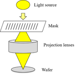
In the lithography process, one of the semiconductor manufacturing processes, it has been necessary to introduce commercial lithography simulation tools to conduct research on Optical Proximity Correction (OPC) and the optimization of both mask pattern and light source, which are required for miniaturization. As a result, it has been difficult for academia to participate in this research. Based on technical support for optics from Tokyo Institute of Technology and Kioxia Corporation, as well as advice on methods for verifying simulation accuracy and improvement measures for acceleration, Masaki Kuramochi, a second-year master's student, and Senior Associate Professor Yukihide Kohira (*1) developed the simulation tool and released it on GitHub (*2). The internal structure of the simulation tool and the results of simulation accuracy verification have been published in IEEE ACCESS (*3).
Amid the challenges in meeting the demand and developing semiconductor personnel, we provide this simulation tool free of charge for use in the education and training of semiconductor engineers in both academic and industrial settings. This will contribute to the acquisition of more practical knowledge and skills in the field of lithography and to the enhancement of the lithography research community.
 |
 |
 |
| Light source shape |
Mask pattern shape |
Optical image on wafer calculated |
(*1) KOHIRA Yukihide Senior Associate Professor


