SCCP-001
SoC Design
Project:1 -
LED with Push Bottom Design on FPGA
Contents
1. Goal
2. Project Creation
3. Compilation of the Design
4. Simulation of the Design
5. Testing Your
Design on FPGA Board
1. Goal
Familiarize
your sef with DE2, Quartus schematic, Simulation, FPGA and Verification
2. Project Creation
Type quartus and click enter
file -->
New Project Wizard
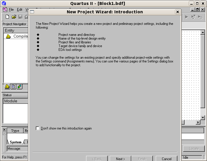
Click next
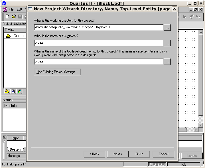
Click next
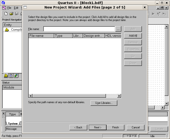
Select the family and device for your
project
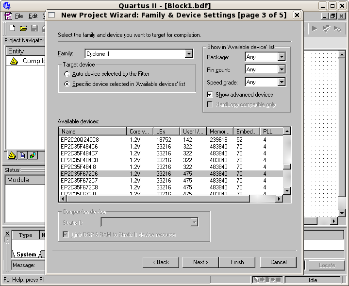
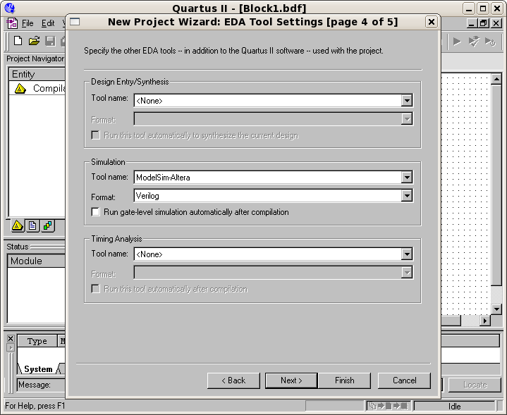
Click next
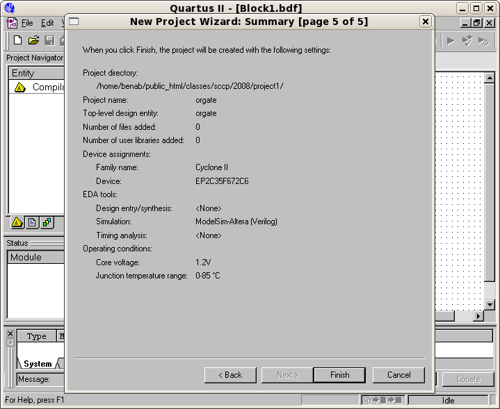
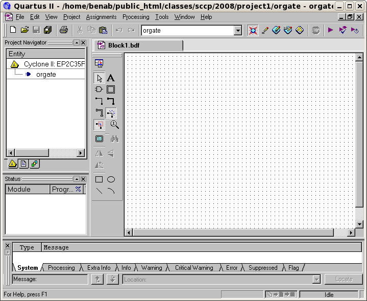
click finish you get this
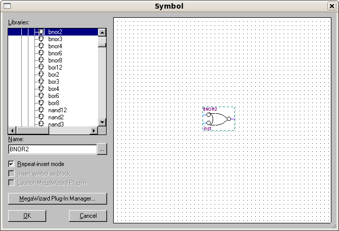
Select BNOR 2
Assigning the input pins for your
schematic
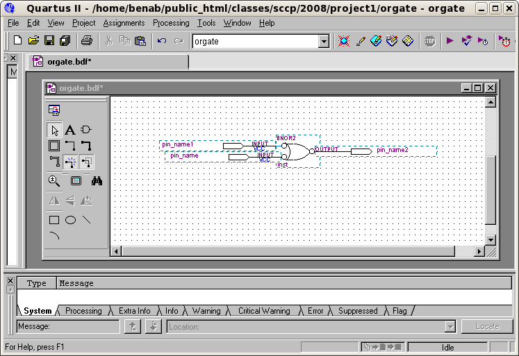
Name the input and output pins
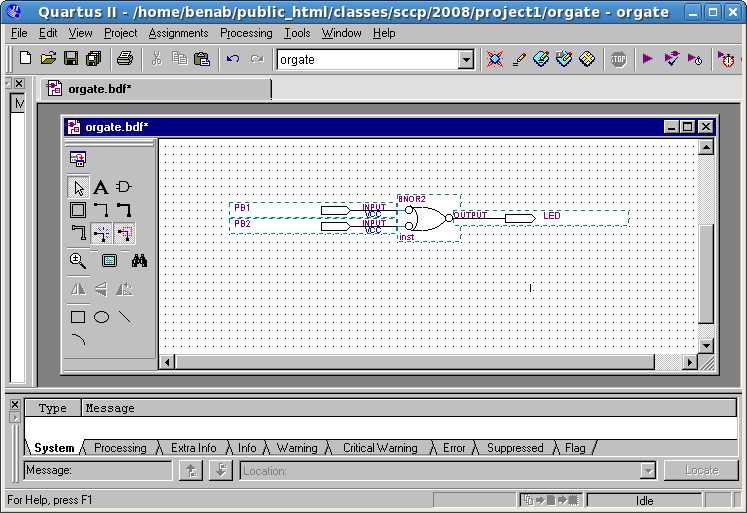
Assign all pins as shown bellow
Save your design file
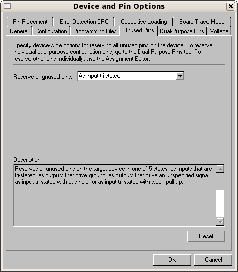
Set Unused Pins as Inputs
Unused Pins --> select the As
input tri-sated option
3. Compiling your design
4. Simulation of the Design
For complex designs, the project is normally simulated prior to
downloading to a FPGA. Although the OR example is simple , we will take
you through the the steps to illustrate the simulation of the circuit.
Set up the simulation trace
Choose file --> New, select
the Other files tab, and then
from the pop up windows select Vector
Waveform File and click
OK.
A bank waveform window should be displayed. Right click on the Name column on the left side.
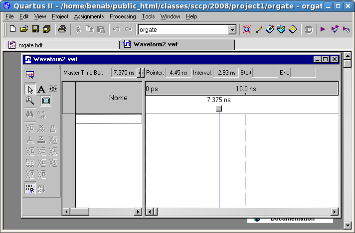
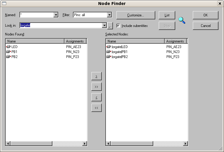
Select Insert Nodes or Bus . Click on the Node finder and then the LIST bottom. LED, PB1, and PB2
should appear as trace values in the window. Then click on the center
>> bottom and click OK
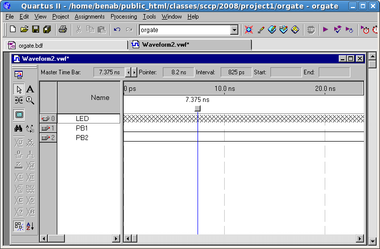
and OK again. The signals
should appear in the waveform window.
Generate test Vectors for Simulation
A simulation requires external input data or "stimulus" data to
test the circuit. Since the PB1 and PB2 input signals have not been set
to a value, the simulator sets them to a default of zero. The 'X' on
the LED trace indicates that the simulator has not been run.
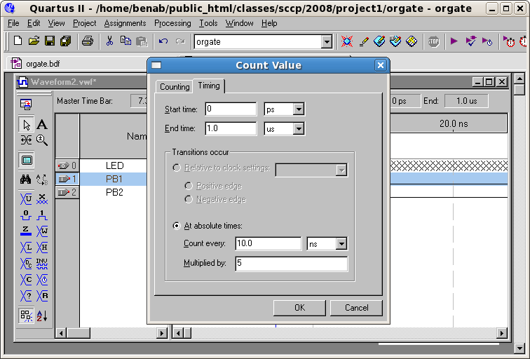
Right click on PB1; the PB1 trace will be highlighted. Select Value --> Count Value, then
click on the Timing tab and
change the entry in the field Multiplied
By from 1 to 5 and
click OK.
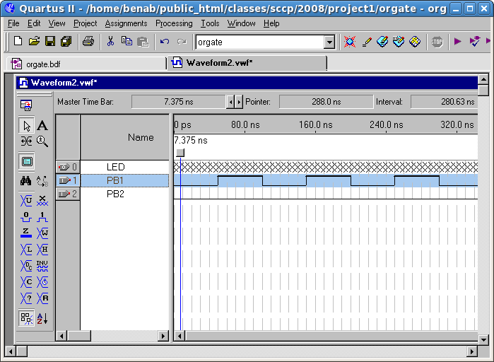
An alternation patterns of highs and lows should appear in
the PB1 trace. (Use View --> Zoom
Out , if you cannot see the pattern)
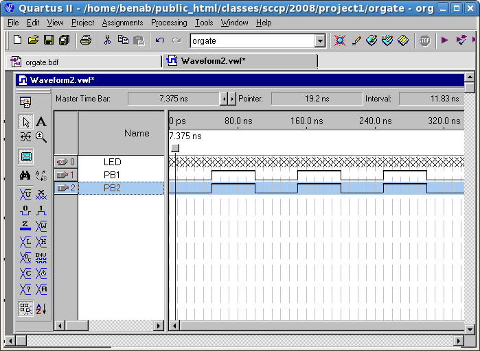
Do the same thing for PB2 . You should get the following windows:
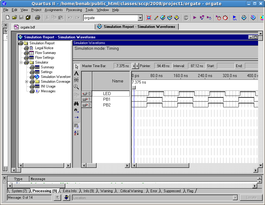
Performing the Simulation with Your
timing Diagram
Select File --> Save
and click Save bottom to save
your project's vector waveform file. Select Processing --> Start Simulation
and click OK on the windows that appear.
5. Testing Your
Design on FPGA Board
The next step is to downland the design to the DE2 board and test it on
real hardware.
Preparing for download
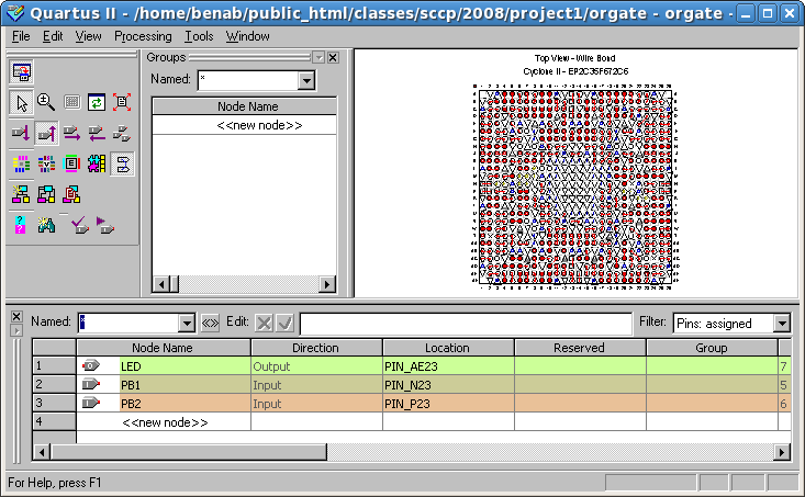
Make sure that you have assigned the correct Device Name for the DE2. The DE2
contains EP2C35F672C6 Cyclone
II FPGA.
When you change the device type you will need also to redo the pin
assignments. Make sure that you have also assigned the correct pin
numbers for the the DE2 board.
Select Tools --> Programmer.
Click on Hardware Setup, select the proper hardware, a USB-Blaster.
Final Steps to Download
The file nem orgate.sof should be displayed in the programmer
window. The *.sof file
contain the FPGA's configuration (programming) data for
your design. To the right of the filename in the Program/Configure
column, check
the Program/Configure box. To
start downloading your design to the board, click on the Start button. Just a few seconds
are required to download. If download is successful , a green info
message displays in the \window notifying you the programming was
successful.
Testing your design
After downloading your program to the DE2 board, the LED in the
lower right corner should turn off whenever a pushbutton is hit. Since
the output of the OR gate is driving the LED signal, it should be on
when no pushbuttons are hit.
Since the buttons are active low, and the BNOR2 gate also has active
low inputs and output, hitting button should turn off the LED.
Congratulations! You have just entered, compiled, simulated,
downloaded a design to FPGA device and verified its operation.
Last update: May 2008